

Summary of the final report of the research project: IGF Project 20144 N – AMPEC
“Additive manufacturing of power electronic circuit carriers”.
The research results of the project AMPEC “Additive manufacturing of power electronic circuit carriers” provide SMEs with a deep and detailed insight into a new technology of additive circuit carrier manufacturing based on selective laser melting. SMEs thus gain access to innovative manufacturing processes for power electronics, which serves as a key technology for a wide range of industries, such as renewable energy technology, the automotive industry and the lighting industry.
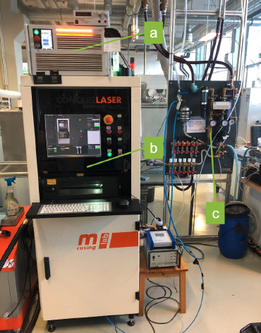
The research project is developing a new technology and alternative to the production of DCB and AMB-manufactured circuit carriers. The production of power electronic circuit carriers requires long process chains with many associated manufacturing steps, such as etching, washing, printing and metallisation processes. Accordingly, a large, cost-intensive plant park is a prerequisite for the production of conventional circuit carriers. As a rule, only large companies are in a position to bear such costs and investments for large-scale production. SMEs are therefore dependent on suppliers and limited in their flexibility of product selection. In principle, SLM technology with the current level of automation and process-related lead times is suitable for small series, prototyping and individual, customer-specific requirements. Further potential savings can be realised in the area of energy and material consumption. The production steps shown in the DCB or AMB process include high energy costs (mainly caused by firing processes) with associated higher material costs and expenses compared to the comparative process due to their subtractive manufacturing character.
In addition, the environmental compatibility of the necessary etching and washing baths is fundamentally debatable. [1] Elaborate disposal measures are necessary, which in turn cause costs. Using the additive metallisation process in selective laser melting, three-dimensional structures can be flexibly applied to the ceramic substrate according to the CAD model. Excess metal powder not processed by the laser can be recycled and reused in the subsequent process. The selective processing of the surface to be metallised by the laser also eliminates the need for the stencils currently used for etching and printing processes.
- Reduction of the equipment required for the production of circuit carriers
- Reduction in the number of production steps
- Significant increase in flexibility
- Shortened time-to-product times
- Possibility of three-dimensional metallisation (bridges, load connections, etc.)
- 2.5 D capability of the substrates
- Reduced environmental impact
- Determination of the bonding mechanism of metal-ceramic joints produced by SLM
- Achieving the maximum possible physical properties of the material composite
You can find more information about the project here.


