LPKF laser direct structuring can be used to efficiently create conductor path structures on three-dimensional components. If there are changes in the circuit layout, all that needs to be done is to adapt the programme. Therefore, LDS is by far the most frequently used method for MID production. Mechatronic Integrated Devices (MID) produced by LDS can be used particularly well for functions such as antenna structures (RFID, NFC), connection technology (connectors, encapsulation) and sensory or optical tasks. In addition, fully functional prototypes can be produced with near-series processes based on the CAD data.
Process Flow
1) CAD drawing
Based on the product idea, CAD data for the plastic base body, the conductor track layout and the assembly are created. All parameters that are decisive for the later component and the manufacturing process are taken into account.
2) Plastic Injection Moulding
The circuit carrier is manufactured in a single-component injection moulding process. A wide variety of specially compounded thermoplastics are available for this purpose.
3) Laser Direct Structuring
In this step, the circuit layout is written onto the component with an IR laser, the surface is ablated at these points and the special active substances (additives) contained in the plastic compound are exposed and activated.
These active substances contain chemically inactive metal nuclei that can only be activated by laser radiation. The slight addition in the plastic compound, the excellent compatibility and the electrically non-conductive properties of these active substances practically do not change the property profile of the applied plastic type. The temperature resistance of the active substances is extremely high, so that no metal release (nucleation) can occur during compounding to the plastic granulate and during injection moulding.
This is then made possible by the structure-writing laser beam, which, by slightly ablating the matrix of the plastic and simultaneously releasing metal nuclei, causes the adhesive strength of the metal layer (base layer mostly Cu) to be far above the norm (0.8 N/mm) after chemical metallisation.
4) Metallisation
During the chemical process of metallisation without external current, a closed conductor track structure is created (typical layer structure: Cu/Ni/Au).
5) Assembly
After the circuit carrier has been completed, it can be used for the usual SMT processes and equipped with the desired components. These can be electronic or mechanical components.
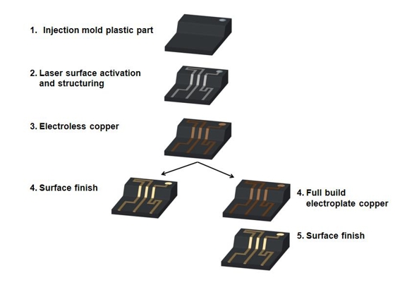
Figure 1: Process flow laser direct structuring; source: 3-D MID
Products
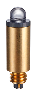
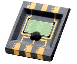
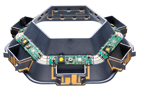
- Constant current source integrated
- LED retro-fit for halogen solution
- Significantly longer battery life
- Miniaturisation
- SMD design
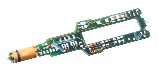
- Integration of fluidic, electrical and mechanical functions
- Integration of sensors and interfaces
- Hybrid solution MID/printed circuit board
- Automated production possible with MID-based bending-resistant modules

- Easy integration into lighting systems
- Plug and play solution
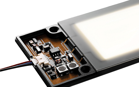
- Glare-free homogeneous surface illumination thanks to integrated electronics
- MID housing as optimal complement to the flat OLED structure
- Connector integrated in MID
- Patient comfort due to slim design
- MID overmoulded with biocompatible thermoplastic material
- 2 variants by adapting the laser program
- Parts can be processed as SMD automatically
- Process simplification through reflow soldering
For further information on MID technologies, please contact the office by phone or by e-mail. See contact details

