

Summary of the final report of the research project: IGF Project 20133 N – 3D Copperprint
“Generative generation of copper tracks by laser sintering on adaptive spatial circuit carriers”
In this research project, the generative printing of copper conductor tracks on three-dimensional circuit carriers for electrical-mechanical hybrid components was developed and investigated as an alternative to existing processes. Together with the focus on circuit carriers from the 3D printer, the project represents a combination of three technology fields: “printed electronics”, “mechatronic integrated devices (MID)” and “additive manufacturing (3D printing)”. Figure 1 visualises the objectives of the project.

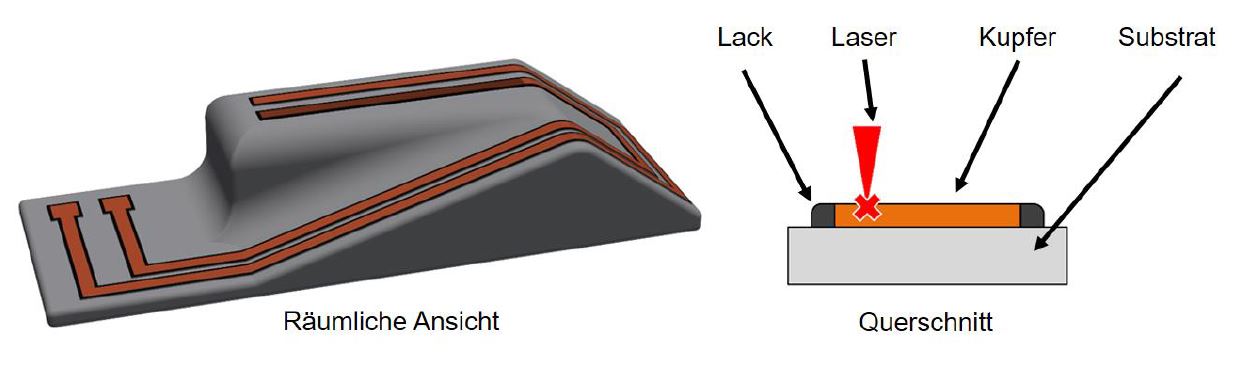
The research approach pursued in the 3D-CopperPrint is based on the application of copper-filled lacquers to the surface of three-dimensional objects and the subsequent laser sintering of the paths. The copper-filled lacquers investigated contain either copper oxide particles or elemental copper particles. Figure 2 shows the process scheme followed. A spatial formwork substrate is coated with copper-containing varnish. Subsequent laser processing makes the copper lacquer conductive and forms the conductor paths.
The basic investigations of laser sintering were studied on 2D samples. After parameterisation with different laser sources, aspects of 3D structuring were then analysed on an industrial laser system from LPKF. The use of this technically more available system technology ensures direct industrial implementation of the research results. The circuit carriers produced were examined for their suitability for further processing with regard to assembly. The scientific questions covered the required pre-treatments and achievable adhesion strengths of the conductor paths on the surface of the circuit carriers, the interaction of the laser radiation with the copper-filled coating and the achievable results in assembly and soldering processes.
In the research project, fundamental questions were determined on several test vehicles. These include injection-moulded components as well as 3D printed components from different printing processes. During the investigations, it became apparent that, especially in the case of components from the 3D printer, there are no well-suited conditions for the laser sintering of thin conductor paths. This is due on the one hand to the often low thermal stability of the plastics used, but also to the fact that the surface roughness of the components is too high. Therefore, a suitable pre-treatment with a primer was developed, which creates suitable properties for the subsequent conductor path generation independent of the component surface. The developed process methodology was then used for the production of a demonstrator. For this purpose, a conductive patch antenna is applied to the inside of an antenna cover from the company “deister electronic” and tested for transmission properties.
Please find more information to the project here.

