

3D optical conductors on functional surfaces using the Mosquito method
Duration: 07/01/2022 – 06/30/2024
Research objective
The research objective of the project is the integration of optical fibers in cavities on 3D surfaces using the mosquito method. In addition, industrial production should be made possible.
Description
In this research project a method for the production of three-dimensional integrated optical waveguides is to be investigated. The waveguides are fully integrated in previously created cavities on a 3D Mechatronic Integrated Device (3D-MID). The so-called mosquito method is to be used to implement this project. This is a method of manufacturing optical waveguides using wet-on-wet dispensing. The light-conducting core is dispensed into a still liquid optical jacket polymer with a needle and the entire structure is then polymerized under UV radiation. This innovative manufacturing process makes it possible to produce both singlemode and multimode waveguides. In this research project, the mosquito method is to be implemented for the first time in cavities on functional MID components. For this purpose, an electro-optical coupling between waveguide and electronics is to be created directly on the 3D component surface. This enables the introduction of optical structures as communication channels (e.g. in MID components), as well as the use by means of optical measurement technology. In addition, integrated lighting elements can be created on 3D surfaces.
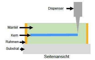
Fig. 1: Schematic representation of the 3D MosquitOPrint process; Source: Leibniz University Hannover, ITA
The addition of optical transmission links in conventional circuits enables a higher data throughput with simultaneous resistance to electromagnetic interference, which is why no additional signal shielding is necessary for the line. In addition, optical transmission links have inherent galvanic isolation that scales with the length of the transmission link (> 3kV / mm). This means that these systems can also be used in environments with high electrical fields and potentially explosive areas. The approach followed also enables the integration of innovative optical measurement technology. One example of this is the integration of Bragg gratings in the waveguides. In particular, temperature and strain sensors should be mentioned here, which can be produced in large numbers at low costs. In order to make this new production technology possible, the following goals are to be achieved within the scope of this research project:
- The additive creation of optical channels directly in cavities on the component. This enables seamless integration into existing processes for the production of 3D components.
- The process should be applicable to various substrate materials with a previously integrated cavity. This is made possible by the fact that there are no special requirements for the surface roughness of the substrates (Rz ≤ 100 μm), since the waveguide cladding is also produced directly additively in the method presented. In addition, non-transparent substrates should also be used (e.g. metals or plastics).
- The diameter of the waveguide (core material) should be less than 10 μm. This is intended to enable the production of single-mode waveguides through the selection of a suitable core-cladding material system.
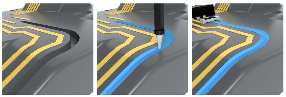
Fig. 2: Schematic representation of a 3D MID with cavity (left), the waveguide generation (center) and the assembled 3D opto MID (right); Source: Leibniz University Hannover, ITA
Economic benefits for SMEs
The worldwide turnover of the German electronics industry is 190 billion euros (2019), which accounts for 11% of German industrial production and thus represents the second largest industrial sector in Germany. Since intermediate goods are mainly manufactured in Asia, there are special opportunities for SMEs in Germany to manufacture specialized industrial goods and offer exclusive services. One possible field of activity is the integration of optical components in electrical 3D-MID components. These can take on sensory tasks as well as be used for the integration of robust high-performance communication in demanding environments, as well as for lighting. These components can then be used in areas that are severely disturbed by electromagnetic radiation, or in areas that require strong galvanic isolation. These highly specialized applications are particularly suitable for SMEs, as they are often small series. An essential part of the technical innovation in this project is the utilization of optical waveguides on electrical circuit carriers. The new product class of optical MIDs creates the basic prerequisites for the development of new types of products. In the composition of the project-accompanying committee (PA), the entire process chain from the manufacture of the products to the use of the products is mapped. New opportunities are opening up, especially for manufacturers of manufacturing systems that are used to produce these components. This gives LPKF (KMU) the opportunity to equip today’s systems with an expanded range of functions and to deliver the new knowledge to its customers in the form of service and training. Manufacturing service providers such as ILFA (KMU) can also use the new process technology for customer orders. In addition, this process also offers manufacturers of injection molding tools, such as Toolcraft (KMU), an entry point into this innovative market, as the cavities for the optical waveguides can be manufactured directly during injection molding. There are new product applications for material manufacturers of polymers such as Jännecke and Schneemann. This creates the potential for higher added value. On the application side, there are just as diverse development opportunities as the increasing demand for components with integrated optical functions from companies such as SIEMENS and HELLA. The demonstrators from this research project are representative of the future need for highly integrated and individually adapted electro-optical products at companies such as SIEMENS and HELLA. On the one hand, an optical sensor plate is to be tested, and on the other hand, the suitability for use in a headlight for automobiles is to be assessed. For applications in the automotive industry, SMEs could act as suppliers of systems for high-volume applications. Due to the high variability of the desired process, there are many opportunities, especially for SMEs, to increase their competitiveness. As a result, typical SME business areas of adaptability, customization and special equipment can be served. The new technology is also suitable for prototyping and small quantities of individualized products, which means that the field of application explicitly overlaps with the business model of many SMEs.
The production of optical 3D-MIDs is a technology that has a high unique value on the market and therefore enjoys a great competitive advantage. Today’s players in the field of 3D-MID technology can use the expansion of the application scenarios to expand their business areas in the future. This enables companies to expand their existing process technology to include a wide range of new products. Due to the free choice of substrate, this process can also be used directly on components made of different materials. This includes metals, ceramics and plastics, as well as composites such as carbon fiber reinforced plastics.
The use of optical measuring or communication technology directly on the surface of large-scale components also simplifies the construction of such systems considerably, since conventional measuring points have to be connected via discrete optical waveguides. In addition, the material consumption can be reduced significantly using 3D MosquitOPrint, so this research also makes a social contribution to environmental protection and improved sustainability.
Research institutes
For further contact details, please contact the office. E-Mail to office
Leibniz Universität Hannover – ITA
Documents
Documents about the project are available in the members area.
If you are not a member yet, you will find information about membership here.
