

Combination of additive manufacturing with printed electronics for personalized products
Duration: 09/01/2021 – 08/31/2023
Research objective
The aim of the research project is to manufacture new types of mechatronic systems by combining MID technology with the possibilities of additive manufacturing. The use of thermally stable thermoplastics in fused layer modeling (FLM) in the base bodies is particularly in focus, as their thermal stability enables them to offer a wide range of applications for individually designed products and the possibility of different post-treatment procedures to optimize the properties – both of the plastic and the integrated conductor tracks – offer. Different placement of conductor tracks in or on circuit boards also enables a comparison between different strand laying processes.
Description
Due to the steadily growing complexity in industrial production, international competition and the globalization of the markets, there is a need for greater flexibility and smaller batch sizes. In addition, individualized products are also becoming increasingly important in the context of Industry 4.0. On the one hand, these requirements can often only be mapped with great effort using traditional manufacturing processes; on the other hand, technical progress in additive manufacturing processes increasingly enables the economical production of small series and individually designed products with relatively high precision and good repeatability. Especially in the field of MID technology (Mechatronic Integrated Devices), for which the requirements in terms of functionality, integration density and reliability are constantly increasing, the additive manufacturing processes offer new possibilities to integrate mechanical, electrical, optical, fluidic and thermal functions. Since MIDs are used in a wide variety of industries, for example in the electronics, automotive, medical and telecommunications industries, there is cross-industry interest. Figure 1 shows the potential advantages that can arise from the combination of MID technology and additive manufacturing. This includes the reduction of the MID process chains as well as possible material and weight reductions that can be achieved through internal recesses. Compared to conventional manufacturing methods, additive manufacturing processes are characterized by short implementation times and tool-free manufacturing and enable significantly higher degrees of design freedom in product design. This is why these are increasingly used today in the series production of metal (e.g. series parts from Audi), ceramic (e.g. sensor holders from Bosch Advanced Ceramics) and plastic components (e.g. spare parts production at Deutsche Bahn, 3Designer from Staedtler). In addition, the competition in the supplier market for processing systems for additive manufacturing is increasing due to expiring patents, new technologies and increasing demand, in particular for strand laying processes such as fused layer modeling (FLM). Over the past few years, this has already led to a sharp reduction in the procurement costs of processing equipment and materials, as well as a widespread use of the technologies. This trend, which will continue in the future, offers unique opportunities for SMEs as well.
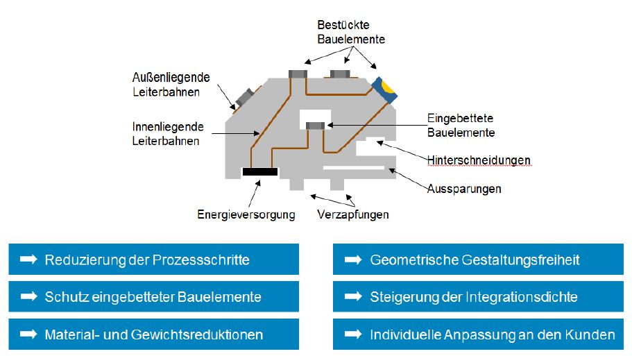
Fig. 1: Scheme of an exemplary EMF with the possibilities of additive manufacturing; Source: SKZ – KFE gGmbH, FAPS
In the strand depositing process, a plastic melt is deposited on a building board. Ideally, this takes place in a temperature-controlled room and is carried out layer by layer until the component is finished and can be removed from the 3D printer. These processes include the trademarked Fused Deposition Modeling (FDM) from Stratasys, which is also known as Fused Filament Fabrication (FFF) or, according to VDI guideline 3405, as Fused Layer Modeling (FLM). Measured by the number of machines sold, these are the most widely used additive manufacturing processes. Both technically and economically, they represent the easiest technology to implement. In addition, a comparatively large selection of materials is available compared to other additive manufacturing processes. The enormous advantages of fused layer modeling already contribute to the fact that besides functional prototypes also individualized products and small series are manufactured and sold. So has z. B. Airbus already approved the FDM for the production of components and was able to develop an unmanned, additively manufactured aircraft in 4 weeks and thereby reduce production costs by 75%. At the 2015 Dubai Airshow, Aurora Flight Science presented the fastest additively manufactured drone (with flight speeds of up to 240 km / h), which was mainly manufactured using the FDM process. The variety and applications of additively manufactured products have increased enormously in recent years and are also reaching the area of 3D-printed electronics. The left side in Figure 2 shows a printed quadrocopter with integrated conductor tracks and components such as B. circuit boards, motors or LEDs. The electronic components are embedded manually during the printing process and connected by conductive silver ink. On the right is a clock with an embedded microcontroller, switches and LEDs. By pressing a button, the flashing LEDs show the time. These case studies show the high potential for additively manufactured EMFs. In the near future, it should be possible to print hearing aids or wearables (portable computer systems) and, thanks to new materials, even lithium-ion batteries. In addition, the customer-specific production of end devices shortens the process chain for the production of mechatronically integrated assemblies.
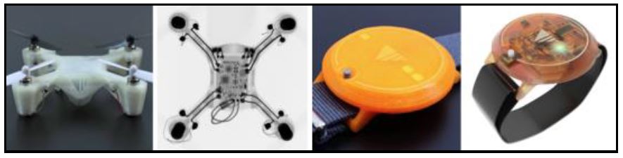
Fig. 2: Examples of 3D-printed MIDs: Quadrocopter (left) and clock (right) with integrated conductor tracks, printed with the Voxel8; Source: 3D Printing Industry, “Voxel8 prints the‘ fun ’in‘ functional ’at CES 2016”, https://3dprintingindustry.com/news/64071-64071/, published on January 5, 2016 [accessed on March 28, 2021]
There is still a high application potential for the use of additive manufacturing in prototype construction. Beta LAYOUT uses additive manufacturing for the construction of base bodies [20]. Subsequent coating with varnish allows circuit carriers to be manufactured using laser direct structuring (LDS), chemical metallization without external current and subsequent assembly processes for components. The prototypes and samples produced in this way are used for functional and layout testing. Due to the high degree of individuality and flexibility of additive manufacturing, a wide variety of customer requirements can be met and specially adapted and optimized solutions can be created. In addition, accessibility is also achieved for individual developers as well as small and medium-sized companies and thus availability for a larger number of users. Additive manufacturing can serve as a catalyst for further innovations and as an important building block for spatial mechatronic assemblies. The project described in the application enables shorter process chains, which increases the profitability of production. Thanks to energy-efficient and resource-saving processes, the use of printed electronics is significantly more environmentally friendly than classic wet-chemical etching and the galvanic construction of circuit boards. Furthermore, fewer different materials are processed, which simplifies disposal and recycling.
Economic importance for SMEs
After more than 25 years of development, the additive manufacturing market is now entering the production phase. Companies along the entire value chain in various industries benefit from this rapidly developing market. In line with the high growth rate of 14.4%, the global additive manufacturing market volume is expected to increase from USD 9.1 billion in 2019 to USD 26.7 billion in 2027.
The 3D printed electronics market is projected to grow from $ 7.8 billion in 2020 to $ 20.7 billion in 2025. The main factors driving the growth of the market include the increased use of printed electronics for the development of intelligent and connected devices, the increase in global demand for energy efficient, thin and flexible consumer electronics, the high demand for flexible new generation printed electronics and the significant cost benefits that printed electronics offer.
The combination of additive manufacturing with printed electronics enables a multitude of new areas of application. Individual electronic products could be completely materialized from their digital description in an integrated hybrid process chain. This would make it possible in the future that, for example, medical hearing aids or sensor / actuator prostheses, portable miniaturized smartphones / watches or wearables can be individually printed out in batch size one. Especially SMEs that are exposed to high economic pressure can make optimal use of the findings from this project and occupy product niches by building up knowledge for the manufacture of additively manufactured MIDs, as well as developing new, innovative business areas and their own manufacturing and product know-how build up. This enables a diversification of the product range, sustainable company growth and thus an increase in the competitiveness of medium-sized German companies. The planned research project directly addresses the requirements of SMEs, which is also reflected in the composition of the project-accompanying committee (PA).
For SME system manufacturers such as Apium Additive Technologies (FLM printing), Neotech AMT (printed electronics) and SEHO Systems (sintering systems), an increasing demand can be expected. Material manufacturers for additive manufacturing (GalloPrint, Headmade Materials) and printed electronics (GSB Wahl) also benefit from this. Manufacturers of highly integrated products such as 2E mechatronic, MID Solutions, Inoptec and Sentinum benefit from the research results in the area of personalized products in MID technology (Mechatronic Integrated Devices).
Furthermore, the planned work can make an important contribution to the methodical approach in the objective evaluation of additive EMFs and ultimately also provide initial approaches to the development of norms and standards. The cross-industry significance of the project results from the diverse areas of application of additive manufacturing and MID components.
Research institutes
For further contact details, please contact the office. E-Mail to office
Friedrich-Alexander-University Erlangen-Nürnberg (FAU)
Institute for Factory Automation and Production Systems (FAPS)
SKZ–KFE gGmbH
