

Dual-cure materials for high-frequency technology
Duration: 01.03.2026 – 28.02.2028
Description
Technological demands in communication systems, security engineering, and radar sensing continue to rise as the trend toward higher operating frequencies intensifies. Conventional planar PCB technology is reaching both economic and technological limits under these conditions. Especially at frequencies above 60 GHz, new approaches are required to improve the electrical performance of high-frequency components such as transmission lines and antennas. In this project, a dual-cure material with an extremely low dielectric loss factor will be developed for additive manufacturing (AM) processes and applied to mirror waveguides, which represent a low-loss signal-transmission technology for printed circuit boards. The developed material system is characterized by excellent adhesion to conventional PCB substrates. In particular, adhesion remains an unresolved challenge for currently available non-polar thermoplastic materials. The manufacturing processes employed will include DLP stereolithography and gel dispensing printing (GDP), whereby the structures are deposited directly onto the PCB surface.
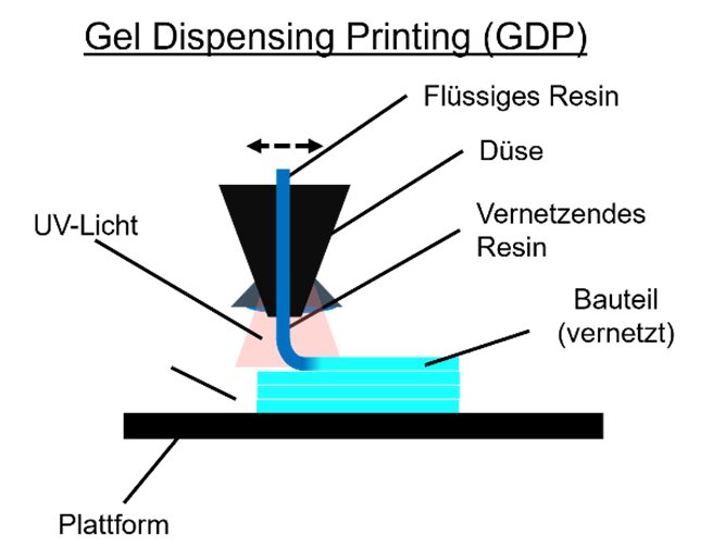
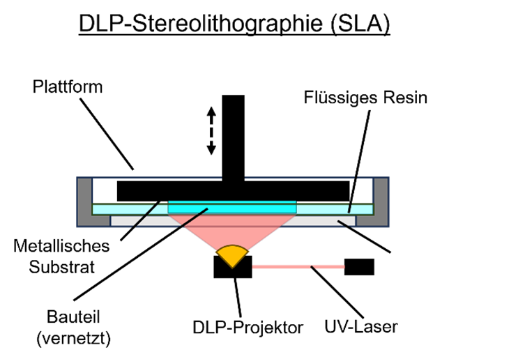
Liquid-based additive manufacturing processes, left – GDP, right – DLP
The investigated dual-cure systems are based on mixtures of low-loss UV-reactive acrylates and thermally latent curing epoxy resins. This enables the fabrication of green bodies during the additive manufacturing process, followed by subsequent thermal curing. Due to the strong chemical interaction between epoxy resins and metallic surfaces, the required adhesion to the PCB substrate is expected to be achieved.
Critical processing-related parameters such as dimensional accuracy, adhesion, and dielectric transmission properties will be identified and characterized within the scope of this project. Based on the acquired knowledge, design guidelines will be derived and a functional demonstrator consisting of a feeding network and three-dimensionally manufactured antennas will be produced.
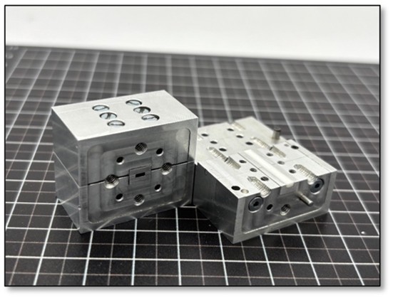
Resonator for dielectric characterization (dimensions: 30 × 18 × 25 mm)
Research Objective
The objective of this research project is to investigate a manufacturing process that enables the direct fabrication or integration of dielectric mirror waveguides onto or into a metal substrate, such as a printed circuit board (PCB). This approach will allow the realization of novel high-frequency (HF) frontend designs consisting of feeding networks and antenna elements. The targeted functionality shall be achieved using dual-cure materials that combine low-loss acrylates with epoxy resins. At the same time, these highly crosslinking materials will be modified with selected low-loss fillers (e.g., polypropylene (PP), polyethylene (PE), and ceramics) to optimize their dielectric properties towards lower losses.
The structures will be manufactured using dispensing-based additive manufacturing (Direct Ink Writing) and vat photopolymerization processes (stereolithography). Through the deliberate use of two different polymerization mechanisms, good material adhesion can be achieved via the epoxy resin component, even for materials considered electrically low-loss (loss factor < 1 × 10⁻³).
For the target frequency range of 40 to 130 GHz, the structural dimensions required for conventional planar stripline technology are typically in the range of 200 to 500 µm. In contrast, dielectric waveguides may feature significantly larger cross-sections of approximately 1–2 mm. This characteristic shall be exploited to enable the most reliable possible integration and fabrication process.
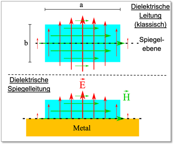
Funktionsprinzip der Spiegelleitung: Die metallische Schicht wird als Spiegelebene für das elektrische Feld innerhalb des Leiters verwendet. Die Höhe der dielektrischen Leitung wird halbiert, während die elektrische Höhe unverändert bleibt.
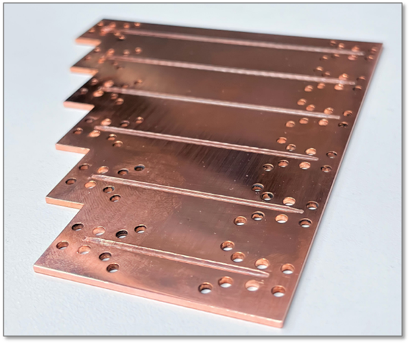
Beispiel des Demonstrators: Kunststoff-Spiegelleitung auf Kupfersubstrat (die Länge der Leitungen ist jeweils von unten beginnend: 40 mm, 50 mm, 60 mm, 70 mm, 80 mm, 90 mm; mit einem Querschnitt von 1 mm).
Benefits and Economic Relevance for SMEs
- Evaluation of the applicability of various material compositions and combinations for the fabrication of high-frequency component
- Additive manufacturing processes enable economical small-batch production as well as rapid and flexible design modifications
- Evaluation of innovative manufacturing methods for three-dimensional HF components provides companies with a technological advantage within the trend of HF technology “moving beyond the PCB
Applications of mirrored transmission lines
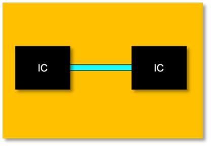
Verbindung zwischen IC-Chips
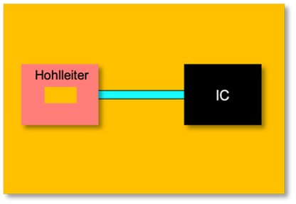
Übergang zwischen Hohlleiter und IC-Chips
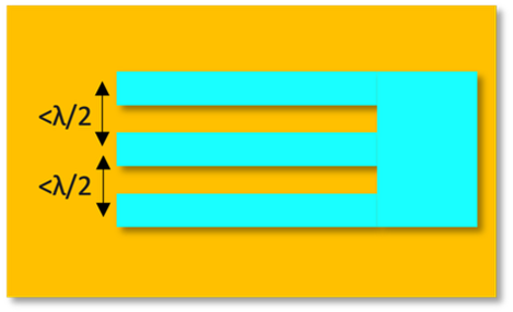
kompaktere HF-Komponente
Research institutes and contact persons
For further contact details, please contact the office (see contact details). E-Mail to office
- FAU Erlangen-Nürnberg Lehrstuhl für Hochfrequenztechnik
- FAU Erlangen-Nürnberg Lehrstuhl für Kunststofftechnik
