

Selective Metallization of 3D Printed Waveguides
Duration: 01.01.2026-31.12.2027
Description
The technological requirements for communications systems, security technology, and radar sensors continue to increase, causing conventional planar printed circuit board technologies to reach their limits. Particularly at frequencies above 60 GHz, new approaches are required to enhance the electrical performance of high frequency components such as waveguides, waveguide transitions, and antennas.
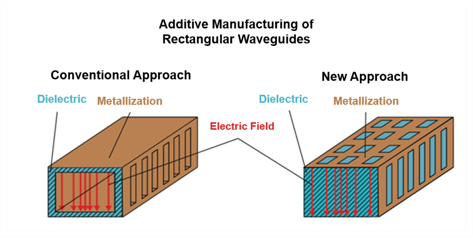
The objective of this project is to develop a manufacturing process for the selective metallization of additively manufactured rectangular waveguides. Through selected structuring of the metallic outer surface, the dispersion characteristics of these waveguides can be deliberately modified, providing significant advantages for applications such as imaging radar systems and high speed communication technologies.
A particular focus of the project is the evaluation and application of various additive manufacturing technologies for the production of high frequency components. The suitability of the following processes for economical low volume production will be assessed: Laser Direct Structuring (LDS), plasma spraying, inkjet printing, Piezojet printing, and Nanojet printing. The fabrication of an E-band (60–90 GHz) demonstrator consisting of feed networks and antenna elements will demonstrate the applicability of the technology.
Additive manufacturing technologies enable economically viable low volume production, allowing smaller quantities to be tailored to specific customer requirements. In addition, these technologies offer a high degree of design flexibility, enabling companies to respond quickly to new requirements and implement modifications with minimal lead times. Furthermore, the evaluation of innovative manufacturing methods for three dimensional high frequency components opens up new opportunities that support the current industry trend of moving beyond conventional printed circuit boards. This provides companies with an important technological advantage and strengthens their competitive position in the growing high frequency technology market.
Benefits and Economic Relevance for SMEs
- Evaluation of the applicability of various additive manufacturing technologies for the production of high frequency components
- Additive manufacturing enables cost effective low volume production as well as rapid and flexible design modifications
- The evaluation of innovative manufacturing methods for three dimensional RF components provides companies with a technological advantage in the ongoing trend within RF engineering to move beyond conventional printed circuit boards
Research institutes and contact persons
For further contact details, please contact the office. E-Mail to office
- FAU Erlangen-Nürnberg Institute of Microwaves and Photonics (LHFT)
- FAU Erlangen-Nürnberg Institute for Factory Automation and Production Systems (FAPS)
